Innovations in PCB Gold Finger Plating Processes


Innovations in PCB Gold Finger Plating Processes
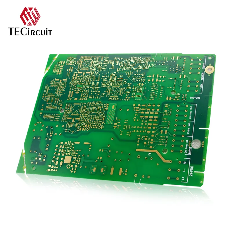
Printed circuit boards (PCB) are an important part in the electronic devices sector. They offer an effective and reliable way for electronic components to interact with each various other. PCB gold finger plating is the procedure of transferring a slim layer of gold onto the subjected copper fingers of the PCB. tecircuit uses numerous advantages, including boosted electrical conductivity, rust resistance, and improved toughness. In this post, we will certainly explore the innovations in PCB gold finger layering procedures that are making it more cost-effective, efficient, and eco-friendly.
Copper Electroplating: The Foundation of PCB Gold Finger Plating
Copper is the foundation of PCB gold finger plating. The copper layer on the PCB supplies the electric pathway between various digital components. tecircuit is the procedure of transferring a thin layer of copper onto the subjected surface areas of the PCB. The copper plating process includes a number of actions, consisting of cleaning, etching, and electroplating. Throughout the cleansing process, the PCB surface area is cleaned up to eliminate any type of pollutants that might disrupt the copper plating process. The etching procedure is made use of to develop the essential copper traces on the PCB. Lastly, the electroplating procedure is used to transfer a slim layer of copper onto the PCB.
The Role of Acid Etching in Preparing PCB for Gold Plating
Acid etching is an essential action in preparing the PCB for gold plating. The acid etching procedure eliminates the slim layer of oxide that develops on the surface area of the copper during the copper plating procedure. This oxide layer can disrupt the bond of the gold plating and impact the electric conductivity of the gold fingers. Acid etching entails the use of a strong acid, such as nitric or hydrochloric acid, to eliminate the oxide layer from the surface area of the copper. The acid etching process is very regulated and needs precise temperature and time setups to ensure that the oxide layer is eliminated uniformly from the surface area of the copper.
Nickel Plating: Connecting Copper and Gold in PCB Gold Fingers
Nickel plating is the process of depositing a thin layer of nickel onto the copper before gold plating. The nickel layer acts as an obstacle in between the copper and the gold. Without nickel plating, the gold would certainly diffuse right into the copper, making it brittle and much less conductive. Nickel plating aids to avoid this diffusion, guaranteeing that the gold layer stays intact which the electrical conductivity of the gold fingers is kept. Nickel plating additionally improves the bond of the gold layer to the copper and boosts the resilience of the gold fingers.
Dual-Layer Gold Plating for Improved Electrical Conductivity
Dual-layer gold plating is an ingenious PCB gold finger plating process that involves the deposition of 2 thin layers of gold onto the copper. The initial layer is a soft gold layer that is transferred onto the nickel layer. The 2nd layer is a difficult gold layer that is deposited onto the soft gold layer. The soft gold layer improves the electric conductivity of the gold fingers, while the tough gold layer gives a long lasting and wear-resistant surface area. Dual-layer gold plating is ending up being progressively prominent in applications where high electrical conductivity and toughness are vital.
Protective Finish: Maintaining the Stability of Gold Fingers
Finally, to maintain the honesty of the gold fingers, a safety finish is used on top of the gold layer. The safety finish works as an obstacle versus ecological variables, such as dampness and temperature level, that can weaken the gold layer and impact the electric conductivity of the gold fingers. The selection of protective covering depends upon the application and running atmosphere of the PCB. Common mixes include nickel/gold, tin/lead, and natural layers.
PCB gold finger plating is a critical process in the electronic devices sector. It provides enhanced electric conductivity, sturdiness, and corrosion resistance. Advancements in PCB gold finger layering processes, such as dual-layer gold plating and protective coatings, are making it more cost-efficient, reliable, and ecologically pleasant. As the demand for high-performance PCBs proceeds to grow, the need for reputable and effective gold finger layering processes will certainly also increase. By remaining updated with the most up to date developments in PCB gold finger layering procedures, electronic makers can make certain that they are meeting the needs of their consumers while keeping top quality standards.